Sections

Left Column
Right Column
Text Area
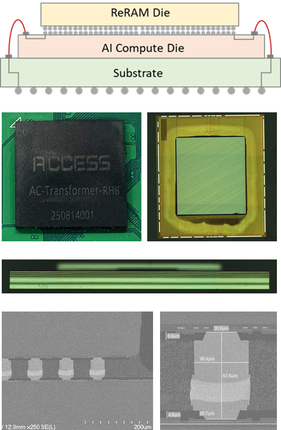
AC-Transformer-RHB: Logic + ReRAM 3D Chip
Text Area
Technology Edges and Chip Highlights
- By adopting CMOS and ReRAM integrated processes, using AI computing chip stacked with ReRAM memory and architectural innovations, effectively reduced both system power consumption and system cost for large model deployment
- Leveraging software-hardware co-design technologies tailored for 3D logic-ReRAM stacking in large model architectures—such as near-memory processing, low-bit quantization, and speculative decoding—achieves an external memory access compression rate of 75–80%
- From 2D to 3D, the global interconnect length of high-density AI computing cores is reduced by more than 50%, while 3D wiring shortens the connection length between ReRAM and compute units by 85%
- Based on co-design methodology and self-developed toolchains, efficient memory management, dataflow scheduling, and instruction parallelism are achieved on multi-core architectures
Text Area
Chip Specifications
| Process node | 55nm LL |
| Metal stack | 1P9M_8Ic_1TMc_ALPA1 |
| Voltage | Core: 1.2V; I/O: 2.5V |
| Data Precision | A: INT8/INT16*/INT32* W: INT8/INT4 |
| MAC# (in main array) | 4,096 |
| Process clock (MHz) | 250 |
| Peak performance (TOPS) | 2 |
| Equiv. NAND2 gates | 10M |
| SRAM Size | 3.4MByte |
| IPs | PLL, ARM M0 |
| Face-to-face bump# | 2912 |
| Bonding pads | 324 |
| Clock domain | 4 |
| Die size | 7mm x 8mm |
| ReRAM Capacity | 8MByte |
| ReRAM Bandwidth | 25.6Gbyte/s (256byte/cycle @100MHz) |
| Package Size | 23mm x 23mm |
Text Area
If you are interested in our technologies, please contact us.